This lab has deliverables to be submitted and marked.
Due date: noon, 3 October 2023, Tuesday
Problem Description:
Most of communication nowadays is done digitally through some computer systems. Errors can happen during the data transmission due to some faults. The simplest of all errors is the error of one bit.
The parity technique is one of the most widely used error detection techniques to detect the 1-bit type of errors.
In the lectures, we have discussed the circuits of the generator and checker of even parity bit for 3 bits of data.
Tasks:
Pre-lab Preparation:
The chip to be used in this lab is one 14-pin quad 2-input XOR gate (SN7486).
This wikipedia page provides a list of 7400 series IC chips and links to their datasheets.
For task 1, the schematic diagram is shown below:
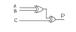
create and fill the pin-out table for this circuit.
For task 2, the schematic diagram is shown below:
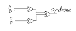
create and fill the pin-out table for this circuit.
In-Lab Tasks:
Wire 2 circuits, one for each task, using the Lab Evaluator, breadboard, one SN7486 chip and wires.
Test your circuits, and demonstrate your circuits to the instructor. Fill the following observation table for each of the circuits. (Note that only the header of the two tables are shown.) These two observation tables should be integrated to your lab report.
| Task 1 Test Cases (for even parity generator of 3 bit data ) | ||||
| Input A | Input B | Input C | Expected Output | Observed Output |
| ... | ... | ... | ... | ... |
| Task 2 Test Cases (for even parity checker of 4 bit data) | |||||
| Input A | Input B | Input C | Input P | Expected Output | Observed Output |
| ... | ... | ... | ... | ... | ... |
(Optionally) take pictures of your circuits and integrate the pictures in your lab report.
The pre-lab preparation and the in-lab tasks can and should be done by a group of up to 2 students.
For the verilog simulation:
Develop two verilog modules using structural method to implement the generator and checker respectively. You can view "xor" as a library function that implements the XOR gate where the first parameter is the output of the gate and the other two parameters represent the two inputs to the gate.
The interface of the two modules are provided in here: parity.v. And if you use the provided interface of the two modules, then here is the test bench verilog file that tests both modules.
What to submit (Deliverables):
How to submit:
You have two ways to submit:
Put all the files you want to submit, the lab report (.txt, or .pdf), the
verilog source code file(s) (.v), and optionally the picture
file(s) (.png), to one directory on any of the cub machines,
then run the following script in the same directory:
~liuh/bin/submit 355 Lab3 .
Alternatively, upload all the files you want to submit to VIU Learn, under CSCI 355's assessment/assignment/Lab 3 tab.