This lab has deliverables to be submitted and marked.
Due date: noon, 26 September 2023, Tuesday
Problem Description:
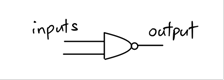
NAND gate (with 2 input and of course 1 output) is a logical gate whose output is false only if both its inputs are true. In other words, NAND gate's output is complement to that of an AND gate. NAND gate's symbol is shown below:
NAND gate is considered to be a universal gate because any other type of gates can be implemented by using NAND gates only.
Tasks:
Pre-lab Preparation:
The chip to be used in this lab is one 14-pin quad 2-input NAND gate (SN7400). You can find this chip's datasheet online here: https://www.ti.com/lit/ds/symlink/sn74ls00.pdf?ts=1694687564294&ref_url=https%253A%252F%252Fen.wikipedia.org%252F. Read especially the section of Pin Function table to get yourself familiar with the chip's layout.
For task 1, the schematic diagram is shown below:
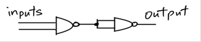
create and fill the pin-out table for this circuit.
For task 2, the schematic diagram is shown below:
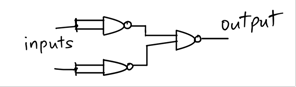
create and fill the pin-out table for this circuit.
In-Lab Tasks:
Wire 2 circuits, one for each task, using the Lab Evaluator, breadboard, one SN7400 chip and wires.
Test your circuits, and demonstrate your circuits to the instructor. Fill the following observation table for each of the circuits. (Note that only the header of the two tables are shown.) These two observation tables should be integrated to your lab report.
| Task 1 Test Cases (for implementing AND gate) | |||
| Input 1 | Input 2 | Expected Output | Observed Output |
| ... | ... | ... | ... |
| Task 2 Test Cases (for implementing OR gate) | |||
| Input 1 | Input 2 | Expected Output | Observed Output |
| ... | ... | ... | ... |
(Optionally) take pictures of your circuits and integrate the pictures in your lab report.
The pre-lab preparation and the in-lab tasks can and should be done by a group of up to 2 students.
For the verilog simulation:
Develop two verilog modules using structural method to implement the AND gate and OR gate respectively using only NAND gate. You can view "nand" as a library function that implements the NAND gate where the first parameter is the output of the gate and the other two parameters represent the two inputs to the gate.
The interface of the two modules are provided in here:implementUsingNAND.v. And if you use the provided interface of the two modules, then here is the test bench verilog file that tests both modules.
What to submit (Deliverables):
How to submit:
You have two ways to submit:
Put all the files you want to submit, the lab report (.txt, or .pdf), the
verilog source code file(s) (.v), and optionally the picture
file(s) (.png), to one directory on any of the cub machines,
then run the following script in the same directory:
~liuh/bin/submit 355 Lab2 .
Alternatively, upload all the files you want to submit to VIU Learn, under CSCI 355's assessment/assignment/Lab 2 tab.